Step-by-Step Guide to Semiconductor IC Layout Design Registration in India
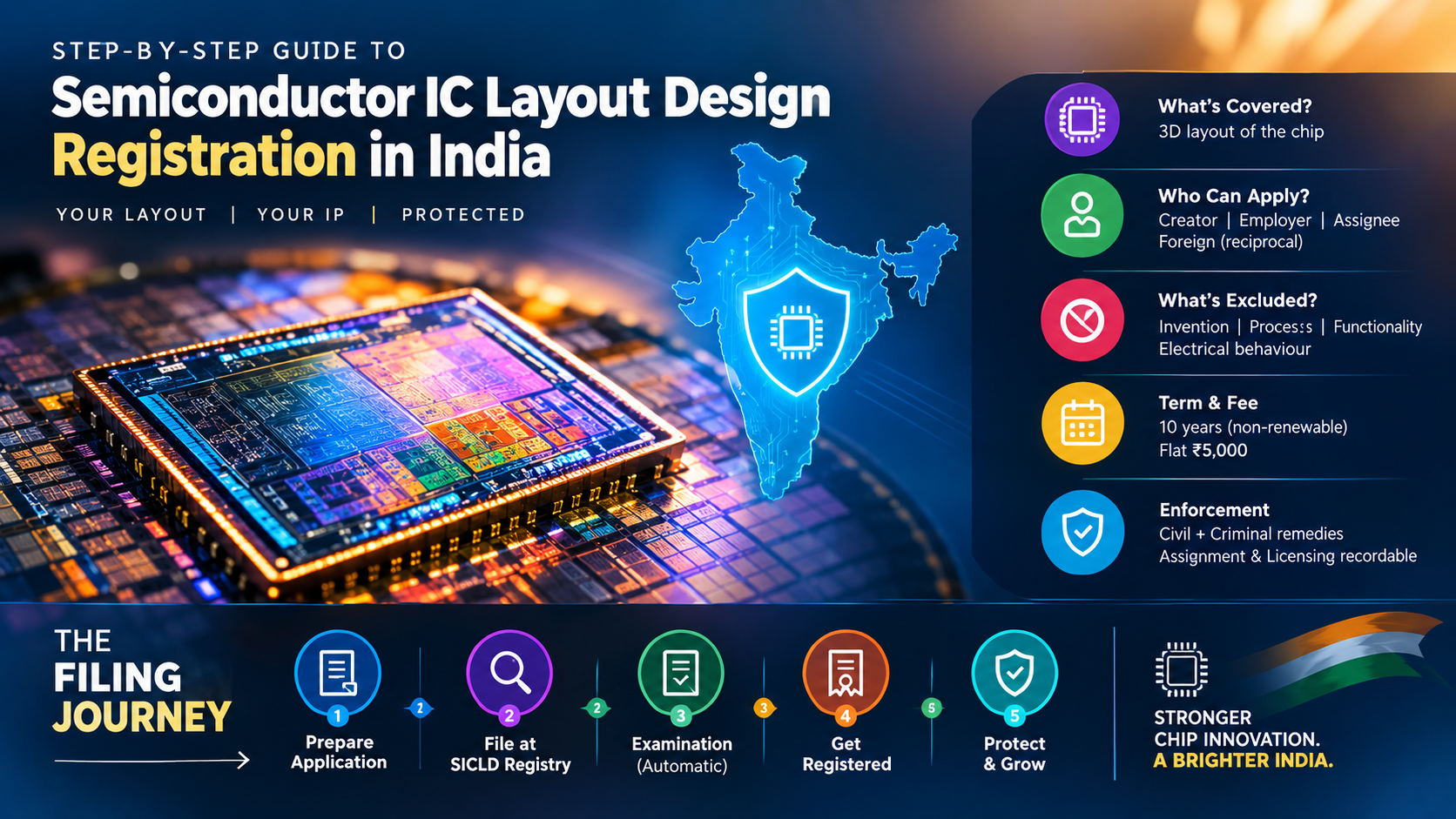
Step-by-Step Guide to Semiconductor IC Layout Design Registration in India
A semiconductor IC layout-design is a three-dimensional pattern of electronic circuitry laid out on the surface of one or more layers of an integrated circuit. India protects this layout, called a mask-work in the foundry industry, under a stand-alone statute that is structurally separate from the Patents Act, 1970, the Designs Act, 2000, the Copyright Act, 1957, and the Trade Marks Act, 1999.
This guide walks founders, IP counsel, and chip-design teams through the Indian filing route that protects the three-dimensional mask-work of a chip: what the law covers, who can apply, what gets excluded, and how an application moves through the SICLD Registry in India.
Step-by-Step Guide to Semiconductor IC Layout Design Registration in India
What is a Semiconductor IC Layout-Design?
A semiconductor integrated circuit layout-design is the topographical arrangement of elements and interconnections that make up an integrated circuit. The protection covers the layout itself, not the underlying invention, the manufacturing process, the underlying functionality, or the electrical behaviour of the chip. The layout-design is a distinct IP asset that sits beside, not inside, the patent and design regimes.
Why is the SICLD Act, 2000 Important?
The Semiconductor Integrated Circuits Layout-Design Act, 2000 was enacted to give Indian chip designers a domestic route to register the layout of a chip without a separate filing in every jurisdiction where the chip is fabricated, packaged, sold, or licensed. The Act takes the sui generis route and creates a dedicated IP right for layout-designs, the same policy framework that the Washington Treaty on IP in Respect of Integrated Circuits (1989) recommends to its contracting parties.
India and the Washington Treaty
The Washington Treaty on Intellectual Property in Respect of Integrated Circuits was adopted in Washington on 26 May 1989 and provides a minimum standards framework for protecting IC layout-designs. As of 13 October 2026 per wipo.int/wipolex/en/treaties/details/treaty_washington, the Washington Treaty has not entered into force, with only three states having ratified or acceded: Bosnia and Herzegovina (8 March 2007), Egypt, and Saint Lucia (18 December 2000). India is not a contracting party to the Washington Treaty. The SICLD Act, 2000, is in this sense a stand-alone national statute rather than a treaty-implementing statute. The Indian filing route is fully independent of the Washington Treaty status.
Objectives of the SICLD Act, 2000
- Provide a sui generis IP right that protects the creative effort invested in an original chip layout, regardless of whether the underlying electronic function is patentable.
- Enable Indian IC designers, fabless startups, and university fab labs to claim a registered IC layout right without overlap or uncertainty against the Patents, Designs, Copyright, and Trade Marks regimes.
- Bring the Indian framework within the policy mainstream that international conventions have recommended since 1989, even where the underlying multilateral instrument has not entered into force globally.
- Reduce the cost of registration by setting a single flat government fee on the principal application form.
Key Features of the SICLD Act, 2000
- Sui generis right. Registration under the SICLD regime does not overlap with patent claims on the chip or with design registration of the chip's casing.
- Originality threshold. The layout-design must be the result of the creator's own intellectual effort and must not be commonplace among creators and manufacturers of integrated circuits at the time of creation.
- Ten-year non-renewable term. Protection runs for a fixed ten-year period from the date of filing or from the date of first commercial exploitation anywhere in the world, whichever is earlier. The registration is not renewable, and the statutory clock cannot be paused or restarted once it begins to run.
- Flat ₹5,000 government fee on Form LD-1. The principal application fee under the SICLD Rules, 2001 is fixed at ₹5,000 for every applicant, with no entity-tier differentiation between natural persons, startups, small entities, and others.
- Automatic substantive examination. Substantive examination by the Registrar is initiated automatically after filing, without any separate examination request.
- Single Registrar location. All SICLD filings are processed at the SICLD Registry housed at Boudhik Sampada Bhawan, Plot No. 32, Sector 14, Dwarka, New Delhi.
- Assignment and licensing recordation. Assignment and exclusive licensing must be recorded with the SICLD Registry to be enforceable against third parties.
- Civil and criminal remedies. Infringement triggers statutory civil remedies and criminal penalties beyond what Patents or Designs alone would offer.
- Reciprocity protection for foreign applicants. Foreign nationals and entities from designated reciprocal countries can file through the SICLD Registry's foreign-filing route.
Who Can Apply?
Any of the following can file an Indian IC layout-design application: the creator, sole or joint; the creator's employer where the layout was created in the course of employment and is the subject of a written assignment agreement; a person who has acquired the creator's rights through a written assignment; and a foreign national or entity from a country with which India has reciprocal arrangements, through the SICLD Registry's foreign-filing route. The applicant categories follow the same creator, employer, assignee, foreign-reciprocal convention found in the Patents and Designs Acts.
Step-by-Step IC Layout-Design Registration Procedure
- Preparing the application package
- Confirm originality of the layout against the commonplace-creator standard before filing.
- Verify the date of first commercial exploitation anywhere in the world, because it controls the operative date of the ten-year term and the Section 7(1)(b) eligibility bar.
- Prepare the prescribed representation of the layout, rendered as a drawing, plot, or mask-work artwork consistent with the SICLD Rules, 2001.
- Prepare Form LD-1 with the creator and assignee identity, country and date of filing, priority-claim data, signature, and the prescribed fee.
- Filing Form LD-1
- Submit Form LD-1 to the SICLD Registry at Boudhik Sampada Bhawan, Plot No. 32, Sector 14, Dwarka, New Delhi.
- Pay the uniform government fee of ₹5,000 on Form LD-1. The fee is the same across all applicant categories under the SICLD Rules, 2001.
- Where priority is claimed from an earlier foreign filing, attach the priority document and a certified translation into English within the prescribed window.
- Substantive examination by the Registrar
- On receipt of Form LD-1, the Registrar places the application on the substantive examination docket without any further action by the applicant.
- Substantive examination is automatic. The applicant does not need to file any separate request for examination.
- The Examiner reviews the application against the originality threshold and the Section 7(1) statutory exclusions, including the two-year commercial-exploitation bar under Section 7(1)(b).
- Reply to examination objections
- The Examiner's first statement of objections is issued in writing.
- Address every objection in writing, point by point, within the statutory reply window under the SICLD Rules, 2001.
- Submit any permissible amendments only within what the SICLD Rules, 2001 allow.
- Registration and certificate
- Once registrability is accepted, the Registrar registers the layout-design on the SICLD Register.
- A Certificate of Registration is issued showing the registration number and the operative date on which the ten-year clock begins.
- Recordation of assignment, licence, change of name
- File the prescribed recordation Form with the SICLD Registry at Dwarka, New Delhi to make assignment, licence, or change of name enforceable against third parties.
- Use the licence and assignment recordation forms prescribed by the SICLD Rules, 2001 in addition to Form LD-1.
Contents of the IC Layout-Design Application
- Form LD-1 carrying the creator and assignee identity.
- Title of the layout-design.
- Number of layers in the layout.
- Drawing, plot, or mask-work representation of the layout-design.
- Country and date of first commercial exploitation anywhere in the world.
- Priority-claim particulars, including country, filing number, and date, where priority is claimed.
- Signature and the uniform ₹5,000 filing fee on Form LD-1.
- Power of attorney where filed through a registered Indian IP agent or attorney.
Validity: The Ten-Year Non-Renewable Term
The SICLD Act, 2000 fixes the protection term at ten years from the date of filing or the date of first commercial exploitation anywhere in the world, whichever is earlier. The term is not renewable. The clock runs once and cannot be paused, extended, or restarted. A defensive filing on the day the chip moves into commercial exploitation elsewhere is therefore structurally preferable to filing the day after, because every day of commerce before the Indian filing date eats into a finite ten-year budget.
What Cannot Be Registered
- Layout-designs that lack the originality threshold and are commonplace among creators and manufacturers at the time of creation.
- Ideas, concepts, discoveries, processes, algorithms, methods, systems, or underlying electrical functions, which belong to the Patents or Copyright regimes.
- Layout-designs of articles that are not integrated circuits as statutorily defined.
- Layout-designs commercially exploited anywhere in the world for more than two years prior to the filing date, excluded under Section 7(1)(b) of the SICLD Act, 2000. This is a hard statutory bar, not a discretionary grace window.
SICLD vs Patents vs Designs vs Copyright vs Trademarks
The SICLD right sits beside four other statutory IP regimes and overlaps with none of them. Layer them deliberately on the same chip: patent on the underlying circuit innovation, design on the chip-package aesthetic, copyright on the design documentation set, SICLD on the layout itself, and trademark on the chip's product mark.
- Patents Act, 1970. Protects inventions (the underlying circuit innovation) for 20 years from the priority date. Filing track is Form 1 plus Form 18 under the Patents Rules, 2003.
- Designs Act, 2000. Protects the aesthetic appearance of an article, for example a chip casing, for 10 years extendable to 15 via Form 3 renewal at year 10.
- Copyright Act, 1957. Protects original authors' works: schematics, mask-shop drawings, and underlying design documentation. Registration is voluntary but evidentiary.
- Trade Marks Act, 1999. Protects the product mark of the chip under TM-A, class-counted per the Nice Classification.
- SICLD Act, 2000. Protects the three-dimensional layout (mask-work) itself for a fixed ten-year non-renewable term under a flat ₹5,000 government fee on Form LD-1.
Why IC Designers Need a Separate Filing Track
Patent protection on an underlying chip invention often takes several years to conclude in India, and patents can be invalidated under Section 3(k) for software-implemented inventions unless the technical-effect test under the CRI Guidelines 2017 is met. The SICLD route takes a different starting point. The layout itself remains a protectable asset even where patent examination has not concluded, where patent claims have been narrowed, or where a Section 3(k) objection has jeopardised patent validity. On the cost side, the flat ₹5,000 fee on Form LD-1 is a fraction of the multi-step fee schedules of the patent and design tracks, and the term carries no recurring fee across the ten-year period.
Section 7(1)(b) and the Two-Year Commercial-Exploitation Limit
Section 7(1)(b) of the SICLD Act, 2000 draws a hard line at two years. A layout-design that has been commercially exploited anywhere in the world for more than two years prior to the Indian filing date cannot be registered. This is not a discretionary grace window; it is a statutory bar. The practical consequence for a fabless chip designer is to file in India well before the second anniversary of first commercial exploitation anywhere in the world.
Conclusion
The right to protect the layout exists in India independent of the Washington Treaty status and independent of patent allowance timing. A defensive filing on Form LD-1 with the flat ₹5,000 fee locks in a statutory priority date and protects the chip layout under a sui generis right that runs for a fixed ten-year non-renewable term from filing or first commercial exploitation, whichever is earlier. Series-B chip designers, Indian fabless startups, university fab labs, and IC design services firms should request a walk-through of the SICLD filing package from a registered Indian IP agent before exposing the layout to commercial partners.